Index
*Introduction
*Fundamental and application of plasmonics
(Research1)
*Current Research in Kyushu University (2011-)
・Nano-Interface Photonics tuned by Metal Nanograin and Nanoparticle
*Research in Japan Science and Technology Agency (JST) PRESTO (2007-2013)
・2009.10 ~ 2013.3 High-Efficient and Ultra-Thin Solar Cells using
・2006.10 ~ 2010.3 Development of super bright light-emitting devices based on plasmonics
(Research2)
*Research in Caltech (2001-2007)
? Development of surface plasmon enhanced light emitting diodes
? Characterization of photonic crystals by near field optical microscopy
? Near field transient lens microscopy of InGaN/GaN quantum wells
? Photothermal molecular sensing by using metal thin-film nano grating
(Research3)
*Postdoctoral Research in Kyoto University (1998-2001)
? Development of the unique laser spectroscopy and apply to several optical materials
? Temporal and Spatial-resolved Nonlinear Spectroscopy of InGaN/GaN
? Spectroscopy of Biological Cell
*Graduate Research in Kyoto University (1992-1998)
? Molecular dynamics of chemical reaction intermediate spaces probed by the nonlinear spectroscopy
Introduction
Nowadays, energy issues became very important problem for us. We spend a lot of energy for illumination at night, so developing high-efficiency light sources is very important to save our energy. Recently, solid-state light-emitting devices have been developed and expected as new-generation light sources because of their advantages such as small, light-weight, long lifetime, easy operation, and saving energy. Since 1993, InGaN quantum wells (QW)-based light-emitting diodes (LEDs) have been continuously improved and commercialized as light sources in the ultraviolet (UV) and visible spectral regions. In 1996, white light LEDs, in which a blue LED is combined with yellow phosphors, have been developed and offer a replacement for conventional incandescent and fluorescent light bulbs. However, these devices have not fulfilled their original promise as solid-state replacements for light bulbs as their light-emission efficiencies have been limited. The most important requirement for competitive LEDs for solid-state lighting is improvement of their quantum efficiencies of light emissions.
Making energy is also very important so much as saving energy. Renewable energies have attracted a great deal of attention as a new energy source instead of fossil resource which is going to be exhausted. The solar energy is one of the most important renewable energy resources and the photocurrent conversion efficiencies of several kind of solar cells have been rapidly developed. Especially, the crystalline solar cells with silicon or compound semiconductors were well developed and their efficiencies were almost reached to the theoretical limits. The drastic cost reduction is much important for such crystalline solar cells to use for much wider areas. For example, making ultra-thin device structures is required to save the materials. On the other hand, amorphous or organic solar cells are very cheap and easy to treat them but the efficiencies are still very low. The improvements of the efficiencies and device lifetime are most important for such solar cells.
A lot of effort and time have been used to improve the efficiencies of LEDs and solar cells, but still it has been very difficult to achieve dramatic improvements. Here I introduce the unique approach to increase these efficiencies based on "Plasmonics". These studies should bring the new application field of plasmonics for green technologies.
Fundamental and application of plasmonics
Conduction electron gas in a metal oscillates collectively and the quantum of this plasma oscillation is called plasmon. A special plasma oscillation mode called surface plasmon (SP) exists at an interface between a metal, which has a negative dielectric-constant, and a positive dielectric material [1]. The charge fluctuation of the oscillation of the SP is accompanied by fluctuations of electromagnetic fields, which is called surface plasmon polariton (SPP). Schematic diagram of the SP and the SPP mode generated at metal/dielectric interface were shown in Fig. 1. The SPP can interact with light waves at the interface and it brings novel optical properties and functions to materials. The technique controlling and utilizing the SPP is called "plasmonics" and has attracted much attention with the recent rapid advance of nanotechnology [2], [3].
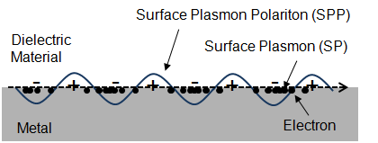
Fig. 1 Schematic diagram of the surface plasmon (SP) and the SP polariton (SPP) generated at the metal/dielectric interface.
The wave vector of the SPP (kSP) parallel to the interface can be written with the following equation when the relative permittivity of the metal is ε1 = ε1' + ε1"i and that of the dielectric material is ε2.
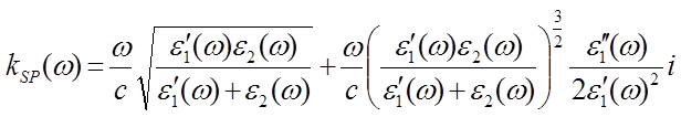
where, ω and C are the frequency of the SPP and the light velocity in vacuum, respectively. The first and second terms of this equation give the dispersion and the damping factor of the SPP. The kSP values are much larger than the wave vector of the light wave propagated in the dielectric media. This fact suggests that the SPP can propagate into nano-spaces much smaller than the wavelength. This enables us to shrink the sizes of waveguides and optical circuits into nano-scale.
Wave vectors of the SPP perpendicular to the interface in a metal or a dielectric material must be an imaginary number because kSP is larger than the light line. This suggests that the electromagnetic fields of the SPP are strongly localized at the interface and it makes giant fields at the interface. This huge field enhancement effect is also one of the most important features of the SPPs. It has been applied to high sensitive sensors using the surface enhanced Raman scattering (SERS), surface plasmon resonance (SPR), and so on.
One futuristic application of plasmonics is the development of high-efficiency LEDs. LEDs have been expected to eventually replace traditional fluorescent tubes as new illumination sources. For example, InGaN-based QWs provide bright light sources, however, their efficiencies are still substantially lower than those of fluorescent lights. The idea of SP enhanced light emission was proposed since 1990, and it has been applied to increase emission efficiencies of several materials which include InGaN QWs. Gontijo et al. reported the coupling of the emission from InGaN QW into the SP on silver thin firm, however they found that the PL intensities dramatically decreased by the SP coupling [4]. By using same sample structure, Neogi et al. confirmed that the recombination rate in an InGaN/GaN QW could be significantly enhanced by the time-resolved PL measurement [5]. However, in these early studies, light could not be extracted efficiently from the metal surface, and the SP coupling has been thought to be a negative factor for LEDs.
Recently, we have reported for the first time large photoluminescence (PL) increases from InGaN/GaN QW material coated with metal thin films [5]. We obtained a 17-fold increase in the luminescence intensity along with a 7-fold increase in the internal quantum efficiency of light emission from InGaN/GaN QWs when nano-structured silver layers were deposited 10 nm above the QWs. We also observed a 32-fold increase in the spontaneous emission rate of InGaN/GaN at 440 nm probed by time-resolved PL measurements [6].
Fig. 2 shows typical PL spectra from an InGaN/GaN QWs separated from Ag films. The PL peak intensities of uncoated samples were normalized to 1 and huge enhancements were observed by Ag coating especially at the shorter wavelength region.
Moreover, we obtained a huge enhancement of light emissions for silicon nanocrystals in silicon dioxide media [7]. Usually the emission efficiencies of such indirect semiconductors are quite low, but by using the SP coupling, it is possible to increase these efficiencies up to values as large as those of direct compound semiconductors.
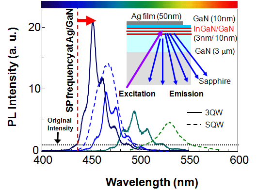
Fig. 2 SP enhanced PL spectra of InGaN/GaN SQW with peak wavelength at 470 and 530 nm (broken lines) and 3QW with peak wavelength at 450, 460, and 500 nm (solid lines) coated with Ag. The PL peak intensity of uncoated sample was normalized to 1. (Inset) Sample structure and excitation/emission configuration..
The SP-emitter coupling technique would lead to high-efficiency LEDs that offer realistic alternatives to conventional fluorescent light sources. However, detail mechanism and dynamics of the SP coupling have been still not so clear. We already achieved efficient blue emissions by using this technique. However, it has been still very difficult to obtain highly enhanced green emissions in spite of the importance of applications of the high-efficiency green LEDs. We try to control the SP coupling conditions by employing the metal nanostructures. Further optimizations of nanostructures should bring highly efficient LEDs and also light receiving devices, namely, solar cells.
[1]. Atwater, H. A., The promise of plasmonics, Scientific American, pp. 56-63 (2007).
[2]. Barnes, W. L.; Dereux, A. & Ebbesen, T. W., Nature, vol. 424, pp. 824-830 (2003).
[3]. Gontijo, I.; Borodisky, M.; Yablonvitch, E.; Keller, S.; Mishra, U. K. & DenBaars, S. P., Phys. Rev. B, vol. 60, no. 16, pp. 11564 -11567 (1999).
[4]. Neogi, A.; Lee, C.-W.; Everitt, H. O.; Kuroda, T.; Tackeuchi, A. & Yablonvitch, E., Phys. Rev. B, vol. 66, 153305 (2002).
[5]. Okamoto, K.; Niki, I.; Shvartser, A.; Narukawa, Y.; Mukai, T. & Scherer, A., Nature Mater., vol. 3, pp. 601-605 (2004).
[6]. Okamoto, K.; Niki, I.; A. Scherer, Narukawa, Y.; Mukai, T. & Kawakami, Y., Appl. Phys. Lett. vol. 87, 071102 (2005).
[7]. Okamoto, K.; Scherer, A. & Kawakami, Y., Phys. Stat. Sol. C, vol. 5, no. 9. pp. 2822-2824 (2008).
(Return to Top)