Currnt Research in Kyushu University (2011-)
 Kyushu University
・Nano-Interface Photonics tuned by Metal Nanograin and Nanoparticle
Nano-interfaces between metallic and dielectric materials bring unique optical properties which can be tuned by nanostructures. Especially, surface plasmons (SPs) generated on metal surface modify emissions, absorptions or scatterings, and produce the complicated optical properties combined with other optical effects. On the basis of this, here we propose a new concept of the nano-interface photonics, which should be applicable to new photonic devices.
For example, we could enhance the emission efficiencies of the various materials by the metal nanograin structures. Fig. 1 shows the enhanced photoluminescence from InGaN/GaN quantum wells with Ag nanograins [1]. The enhancement ratios depend on the grain sizes because the grains act as the nanogratings. By using this, we can excite the propagating SP polariton mode without the periodic nanograting structures fabricated by top-down processes. This method should be useful to develop the higher efficiency light-emitting devices (LEDs).
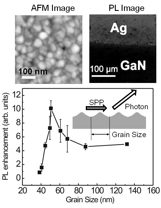
Fig. 1 PL enhancements with Ag nanograin structures.
Metal nanoparticle two dimensional sheets are also very promising structures for various applications. We could control the localized SP resonance spectra with much wider wavelength regions by employing the nanosheet of Ag nanoparticles with 5nm diameter. Moreover, We succeeded in more flexible and remarkable tuning of the resonance spectra by making the multilayered Ag nanosheet structures on metal substrates [2] (Fig. 2) This effect should originate not only from the near-field SP resonance but also from other far-field optical effects at the multilayered nanosheet. This technique should be useful to develop the sensing technologies, the light harvesting for the solar cells, and also the full-color painting. The detail mechanics of the tunable optical properties with nanosheets will be discussed at the conference.
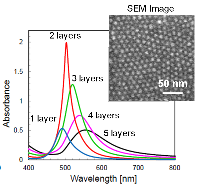
Fig. 2 Tuning of resonance spectra with multilayered Ag nanoparticle sheets.
Flexible tuning of the SP resonance within the visible wavelength range was already achieved by using several metallic nano-structures as described above. Next important challenge is extension of the SP resonance range into UV or IR wavelength regions. To extend plasmonics tuning into DUV regions, Al should be useful because the SP resonance frequency of Al is located at the DUV region (~200nm). We fabricated the nano-grain structures of Al and succeeded in 7-times enhancements of DUV (~250nm) light emissions from AlGaN/AlN-based QWs with Al [3].
We used Al as a metal SP arises on also for wider visible wavelength region. We obtained remarkably enhanced photoluminescence (PL) spectra with Al and shown in Fig. 3 [4]. The PL enhancement ratios for blue and green emissions were 150 and 80, respectively. These ratios were much larger than those with Ag films. We estimated the internal quantum efficiency (IQE) of emission by assuming IQE~100% at the low temperature. We also measured the PL time profile by the time-resolved PL measurements. We found that neither IQE nor spontaneous emission rate was improved with Al. These results were quite different from the previous results with Ag, and suggested that the obtained PL enhancements should be due to the improvement of the absorption of the excitation light by the SP resonance. The obtained property of the SP resonance on Al should be suitable to apply to the efficient photo-detectors or solar cells.
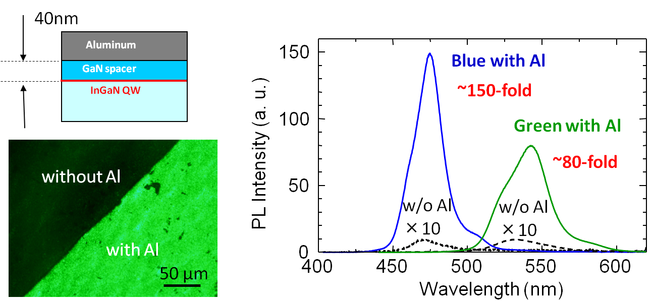
Fig. 3 PL enhancements of InGaN/GaN QW with Al nanograin structures.
On the other hand, to extend plasmonics into IR wavelength region has been very difficult because the many kinds of metals have large dumping factors of the dielectric constants at the IR regions. Recently we fabricated the nano-sheet structures by using Au nano-particles, and achieved the flexible tuning of the SP resonance at the NIR regions [5]. Moreover, we found that some metals such as Ta or W have a potential to have the SP resonance at the longer NIR wavelength regions by the finite-difference time-domain (FDTD) calculations.
These methods to Tune the SP resonance over the DUV-NIR range should bring new possibilities of applications to plasmonics. We believe that our approach of device applications based on tunable plasmonics would lead to new class of several photonic and electronic technologies.
[1]. X.-Y. Xu, M. Funato, Y. Kawakami, K. Okamoto, and K. Tamada, Opt. Exp., 21, 3145 (2013).
[2]. K. Okamoto, B. Lin, K. Imazu, A. Yoshida, K. Toma, M. Toma, K. Tamada, Plasmonics, 8, 581 (2013).
[3]. A. Takada, T, Ohto, R. G. Banal, K. Okamoto, M. Funato, Y. Kawakami, Meeting of JSAP (2010).
[4]. K. Tateishi , X.-Y. Xu, M. Funato, Y. Kawakami, K. Okamoto, K. Tamada, 7th International Conference on Molecular Electronics and Bioelectronics, Mar. 2013
[5]. A. Yoshida, K. Imazu, X.-H. Li, K. Okamoto, and K. Tamada, Langmuir, 28, 17153 (2012).
(Return to Top)
Research in Japan Science and Technology Agency (JST) PRESTO
 Science and Technology Agency (JST)
・High-Efficient and Ultra-Thin Solar Cells using Plasmonics
This project aims to achieve dramatic improvements of photoelectric conversion efficiencies and reductions of costs by thinner solar cells by using new approach based on plasmonics. It is expected to realize a first practical use of plasmonic solar cells by using our original technique which we developed to enhance light emission efficiencies by plasmonics. Surface plasmon (SP) generated between dielectric/metal interfaces can well increase the efficiencies of light emission and photoelectric conversion. This effect should be applicable to high-efficiency LEDs and solar cells. Recently, for the first time, we reported the SP enhanced emissions experimentally [6].
Fig. 4 shows the energy conversion scheme of the SP coupling and light emission. The SP-exciton and SP-photon coupling processes provide new emission pathways. The high efficiency LEDs should be achievable if the new emission path through the SP coupling is much faster than the original emission path [ ( (3) > (2) +(11), (4) > (12) in Fig. 4].
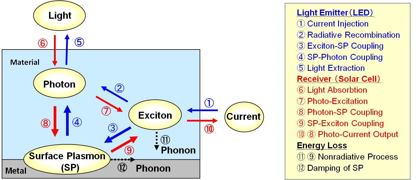
Fig. 4 Energy conversion schemes of the SP enhanced LEDs and solar cells.
By the similar way, plasmonics should be also able to improve high-efficiency solar cells, because the SP-exciton and SP-photon coupling processes are reversible. The sun-light can couple to the SP at the metal/dielectric interface and generate the excitons in the dielectric materials. This process should increase efficiencies of light absorption and photocurrent conversion if (8) > (7), (9) > (12) in Fig. 4. The plasmonic solar cells based on such photon-antenna effect have been already reported. For this project, we also try to optimize the SP-exciton coupling in order to achieve much higher efficiencies. We also try to tune the SP coupling conditions by using several metal nanostructures, and proposed the new type of plasmonic solar cells (Fig. 5).
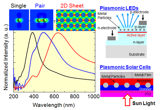
Fig. 5 SP resonance spectra and possible device structures.
[6]. K. Okamoto, I. Niki, A. Shvartser, Y. Narukawa, T. Mukai, and A. Scherer, Nature Materials, 3, 601 (2004).
[7]. K. Okamoto, Y. Kawakami, IEEE J. Select. Top. Quantum Electron. 15, 1190 (2009).
・Development of super bright light-emitting devices based on plasmonics
Nanophotonics and Plasmonics have attracted a great deal of attention and are expected to be at the forefront of new optical and electrical technologies for the next generation. For example, photonic crystals enable us to control light wave flexibly beyond the diffraction limit. Surface plasmons also offer the unique ability to localize and enhance electromagnetic fields. Surface plasmons are special type of electronic vibrations generated at metal interfaces that can be controlled by fabricating nanometer scale structures. One futuristic application is the construction of super bright light-emitting devices that would replace conventional light sources. Part of this expectation has been realized in the form of Solid-state light-emitting devices, however, emission efficiencies and cost performance of these solid state devices need to be improved. My project tries to work towards this goal by developing super bright light-emitting devices using surface plasmons. Recently, we invented a novel method to enhance this light emission efficiency by using surface plasmon coupling with fabricated nanostructures. We found that this technique increases both the spontaneous emission rates and the internal quantum efficiencies. I believe that this technique will provide a route for an early realization of the "illumination revolution" with super bright solid-state devices replacing conventional incandescent and fluorescent light bulbs. Such efficient and high-speed optical devices would in turn make possible desirable new technologies such as optical logical circuits and optical computing. My research also includes the development of advanced optical measurement techniques to characterize and understand nanophotonics and plasmonics. I have developed unique spectroscopic techniques with high spatial and time resolutions based on the scanning near-field optical microscopy and the third order nonlinear optical spectroscopy. These developments will provide new tools to understand the underlying physics as well as the help in the engineering of more efficient light emitters.
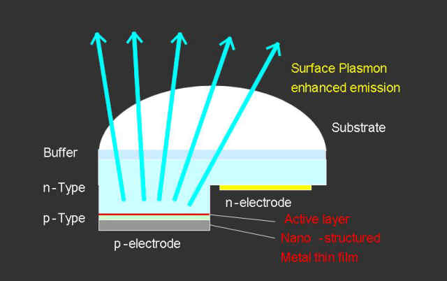
Fig. 6 SP Super Bright Plasmonic LED
These works provide a foundation for the rapid development of highly efficient and high-speed solid-state light emitters. First, our proposed super bright LEDs would bring the “illumination revolution” to fruition, i.e., finally replace Edisonian light bulbs and fluorescent tubes with solid state light emitters as the dominant white light sources. Second, by using our developed optical characterizing technique, the detailed mechanisms and dynamics of plasmon optics and nanophotonics could be clearly understood. This should result in much more efficient and advanced optical devices. We also propose some new plans to use geometry to control the behavior of photons on the microscopic scale. In short, our project will result in very important and fundamental work for developing the underlying physics for enabling future photonic technologies.
The development of highly efficient and high-speed solid-state optical devices would enable highly desirable new technologies in near future. For example, now the applicant holds US-patent (US-6,629,762) and a corresponding Japanese patent for the idea and theory for a 3D holographic movie player/recorder using nano-structured electric field sensors. This idea represents very interesting and important future technologies but has been so far very difficult to realize. Therefore, 3D holographic movies have not so far been realized and exists only in science fiction. As this new technique needs a super bright light emitters, high-speed optical modulators, and nano-sized structures of liquid crystal cells. We believe that it could be realizable by gathering the nanofabrication techniques and the thus the results of this project could impact even Hollywood.
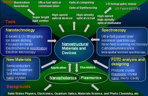
Fig. 7 Future Plans of Plasmonics Research
(Return to Top)