Research in Caltech (2001- 2007)
 California Institute of Technology
? Discovery and analysis of surface plasmon enhanced light emission
Since 1993, InGaN light emitting diodes (LEDs) have been improved and commercialized as light sources in the ultraviolet and visible spectral regions, but their original promise as solid-state replacements for light bulbs has so far been delayed as their light emission efficiencies have been limited. The most important requirement for a competitive LED for solid-state lighting is the development of new methods to increase its quantum efficiency of emission.
Quite recently, we invented a novel method to enhance this light emission efficiency by using the coupling between surface plasmons (SPs) and quantum wells (QWs). SPs offer the unique ability to localize, extract and enhance electromagnetic fields. So far, the actual enhancement of light emission by SP-QW coupling had not been observed directly in visible spectral region. We found for the first time a significant SP enhancement of light emission from InGaN/GaN with metal layers deposited 10nm above the QWs. As the photoluminescence (PL) peak of the uncoated wafer at 470 nm was normalized to 1, it is clear that dramatic enhancements in the PL intensities from Ag and Al coated samples can be obtained. No such enhancements were obtained from samples coated with gold, as its well-known plasmon resonance occurs only at longer wavelengths. We also showed that SP-QW coupling actually increase the internal quantum efficiency (ηint) of emission by measuring the temperature dependence of PL intensities. These ηint values increased 6.8 times (to 41%) with Ag and 3 times (to 18%) with Al, explainable by spontaneous recombination rate enhancements. These surprisingly increasing of emission efficiencies suggests that SP enhancement of light emission from InGaN QWs is a very promising method for developing the super bright LED devices, which emission efficiency should be also over 6-hold larger than that of presents.
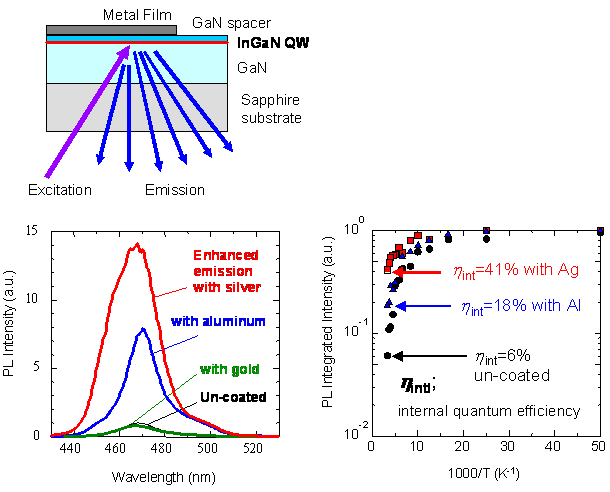
(Left) Surface plasmon enhanced PL of InGaN/GaN quantum QWs. (Right) Temperature dependence of PL
We propose to fabricate the super bright LED structures by using the SP-QW coupling. In order to design and fabricate even more efficient optical devices for wider spectral range, we have to understand and optimize the mechanism and dynamics of SP-QW coupling and light extraction. We will test several nanostructures of metal layers and the dependence of various metals includes mixture metals, thickness and grain shapes/sizes of metal layers. Until now, a lot of efforts to increase the emission efficiency have been investigated based on the development of the crystal growth techniques, but, there are limited. Our SP-QW coupling method is one solution to increase dramatically the efficiencies of InGaN/GaN LEDs. The following figure shows the historical development of solid-state light emitters. We also plotted the expected efficacy of our super bright InGaN/GaN LEDs. We estimate that the increasing of the internal quantum efficiencies of emission is at least 2-fold and increasing of the light extraction efficiency is also at least 2-fold from those of the present best InGaN LEDs. Therefore, our proposed LEDs are expected to achieve extraordinary high efficiency (120lm/W) beyond that of the fluorescent tube (75lm/W). Our super bright LEDs can provide the evolutional rapid development of solid-state light sources taken place the present light sources (fluorescent tube or light bulb).
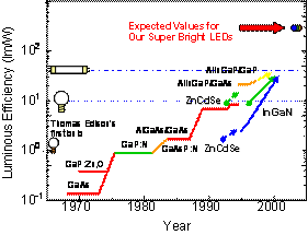
Historical development of the luminescence efficacies of LEDs and expected values of our super bright LEDs.
? Characterization of photonic crystals by near field optical microscopy
Recently, near-field scanning optical microscopy (NSOM) has been used as a powerful alternative method to analyze local electromagnetic field distributions in fabricated nanophotonic structures. Several groups have reported NSOM studies of planar photonic crystal (PPC), however, high spatially resolved near-field images of the field distribution inside the PPC cavity have not so far been reported. We succeeded for the first time to observe the optical mode images obtained by NSOM on very small PPC cavities based on fractional edge dislocations. A cw light from a He-Ne laser (633nm) and a 20ns pulsed diode laser (780nm) were used as the excitation laser source for illumination mode (I-mode) and the collection mode (C-mode) measurements, respectively. Photoluminescence (PL) signals were distinguished from the excitation laser by using the colored glass filter with a cut-off wavelength of 850nm, and detected with a high-sensitivity (fW) InGaAs photo-detector. The metal-coated fiber tip, with small aperture size, enables us to distinguish between localized cavity modes and propagating far-field modes, and to obtain more precise mode profiles when the tip probes into holes of photonic crystals. The best resolution in our system is as small as 50nm. By using the shear-force detection, we could also obtain a topographic image of the sample, in addition to the near-field optical image. We have also performed micro photoluminescence measurements on our structures in order to confirm the existence of the localized cavity modes. The photonic crystal nanocavities fabricated in active InGaAsP material used in this work are very similar to those used to realize low-threshold lasers described in our previous publication. We have observed localized defect modes of the compact photonic crystal nano-cavities by using I-mode. The size of the detected mode was roughly four by three lattice spacings. To the best of our knowledge, the optical modes and field distribution that we have observed are the smallest reported so far. High-resolution near-field optical images were obtained by using a metal-coated optical fiber tip with a 150nm aperture size. In addition to localized cavity modes, we have observed dielectric band modes in bulk photonic crystals surrounding the nanocavity by geometrically altering the bands in emission range and eliminating localized modes out of the emission range by using C-mode. The confined cavity modes observed by near-field microscopy were confirmed by micro photoluminescence experiments, and very good agreement between the two analysis methods was found. We conclude that near-field scanning optical microscopy is a powerful tool for investigation of local profiles of confined modes in nanocavities.
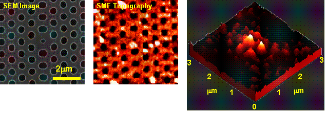
NSOM Image of photonic crystal laser
? Near field transient lens microscopy of InGaN/GaN quantum wells
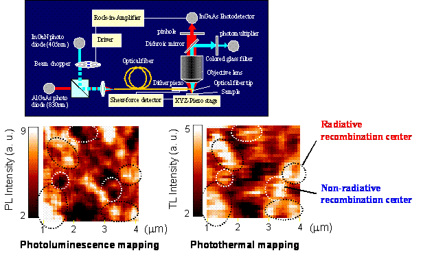
We developed two-beams NSOM measurements based on the transient lens effect, which provides a third order nonlinear optic signature for carrier properties in semiconductors. By using this meted, we succeeded to observe the non-radiative processes, for example, carrier diffusion/ recombination, phonon generation, or heat conduction in InGaN/GaN. Such processes are also important effects dominating the optical properties of light emitters, but have proven to be very difficult to observe experimentally by traditional optical measurements. We obtained the near-field PL image and TL image of InGaN/GaN at room temperature with time-modulated (400Hz) InGaN laser (405nm) and a AlGaAs laser (830nm) as pump and probe beams, respectively. We obtained the topography, reflection, PL and TL images of the InGaN/GaN at the same time. We found a sub-micron scale spatial inhomogeneity in the near-field image of both PL and TL signals. Spatial inhomogeneities of PL intensities and peak wavelengths in InGaN/GaN QWs were previously reported and interpreted to be a result of fluctuations of the indium composition, the QW thickness, and the piezoelectric field in InGaN active layers. These fluctuations are very important and may act as the carrier localization centers, and suppress the pathways for nonradiative recombination of carriers. Such carrier localization has been known as one of the reasons for the strong emission properties in InGaN/GaN materials. In this study, we found that the NSOM-TL image was also distributed inhomogeneously on a sub-micron scale. This suggests that the nonradiative carrier processes (diffusion, localization, or thermalization) should also be spatially distributed at submicron scales. We also found a strong correlation between the PL and TL images. Under this condition, the carrier density signal represents the main component in the NSOM-TL signal. Therefore, the TL images can be used to represent the carrier density in active layers and the bright region should correspond to the carrier localization areas. By comparing the PL and TL images, it was found that the many bright regions in the TL images correspond to the bright regions in the PL images. In these regions, carrier localized areas are well act as the radiative recombination (emission) centers. On the other hand, some bright TL regions correspond to the dark region in the PL image. We believe that these regions should be represented to the nonradiative recombination (thermalization) centers of carriers in the materials. To the best of our knowledge, this is the first report of the direct mapping of the distribution of the carrier density and the nonradiative recombination in InGaN/GaN-based optical devices. Such results are important to understand the carrier dynamics and the emission mechanism in InGaN but could not be obtained with previous spectroscopic techniques. In conclusion, the Near field transient lens microscopy is powerful method to characterize LEDs or other optical devices.
? Photothermal molecular sensing by using metal thin-film nano grating
Recently, microfluidic technologies have been developed and applied widely in biology and analytical chemistry. The fluorescent latex beads, DNA with fluorescent dyes, or colored solutions have been used as the host objects in such fluidic channels. However, many molecules and chemical compounds have neither color nor fluorescence/phosphorescence. High sensitive molecular sensing technique without human visibility is necessary for chemical and biomedical applications of microfluidic devices. In this article, we propose the highly sensitive molecular sensing technique based on the third order nonlinear spectroscopy with nano and micro-metal gratings fabricated in our laboratory in order to apply to the monitoring of the microfluidic devices. Time-modulated InGaN laser or a frequency-tripled Nd:YAG laser (355nm) was pump beam. A cw-He-Ne laser (633 nm, 0.05 mW) was used as probe beam. Both beams were focused by a lens at the fabricated metal grating in sample solution. Diffracted probe beam was isolated with a pinhole and a glass filter and detected with a InGaAs photodetector. Nano and micrometer scaled metal gratings were fabricated by chromium evaporation on quartz substrates, patterned by electron beam lithography, and chemical etching. Sample solution which we used was nitrobenzene in 2-propanol (5 volume %). Nitrobenzene is not colored and has neither fluorescence nor phosphorescence, so molecular detection of nitrobenzene has been very difficult. We obtained the diffracted signals which have two components; the large background offset component (Ir) and the time modulated signal component (Is). According to the nonlinear optics theory, proportional relationship is obtained between Is(t) and the refractive index change [δn(t)] induced by the temperature grating and density grating at this frequency scale (100 Hz). Then, Is is proportional to the molecular concentration. This suggests that the solute molecular concentration can be detected by this technique. In order to observe the actual time dependence of the relaxation of transient grating, we investigated the time-resolved measurement. Obtained signal decay times were reasonable to those values calculated by the thermal diffusivity in solvent. This excellent agreement shows the validity of the signal analysis method. In conclusion, we developed the new technique of the third order nonlinear optical spectroscopy by using the fabricated nano and micro gratings. This method has many advantages compared with traditional techniques; (1) simple setting and easy alignment, (2) high sensitivity and high S/N ratio (heterodyne detection), (3) high speed (high frequency) detection, and (4) easy analyzing (linear relationship between signal intensity and molecular concentration). This technique is expected to be a powerful tool to monitor the molecules in nano and microfluidic devices.
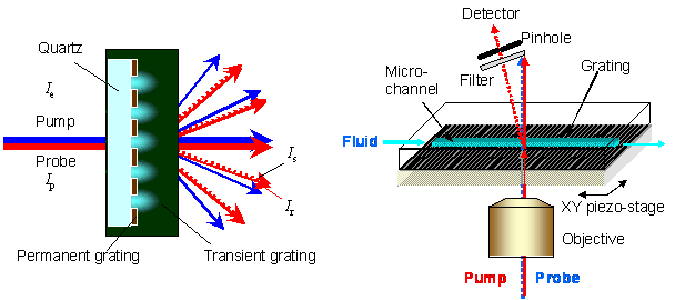
Molecular sensor by using nano-grating film in microfluidic devices
(Return to Top)